| Definition |
Prototype PCB board |
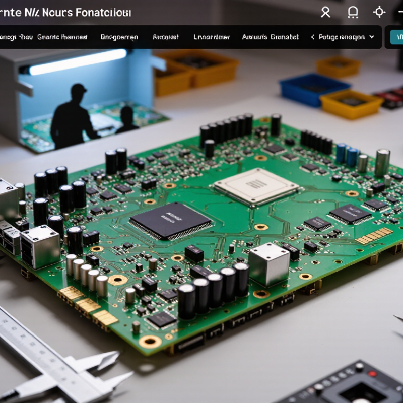
A trial printed circuit board produced to verify circuit design, component placement, electrical performance, and manufacturability before volume production. |
It helps identify design and assembly problems at an early stage. |
| Primary Purpose |
Design validation |
Testing electrical function, mechanical fit, thermal behavior, signal integrity, and assembly procedures. |
Validation reduces the risk of costly changes after production begins. |
| Common Layer Count |
Board structure |
Single-layer, double-layer, and multilayer constructions are commonly used for prototypes. |
The required layer count depends on routing density, power distribution, grounding, and signal requirements. |
| Base Material |
Substrate |
FR-4 glass-reinforced epoxy laminate is widely used for general-purpose rigid prototype boards. Flexible prototypes may use polyimide. |
The substrate affects rigidity, thermal performance, dielectric properties, and fabrication cost. |
| Conductive Material |
Copper layer |
Copper foil forms the conductive traces, pads, planes, and plated connections. |
Copper thickness influences current-carrying capacity, resistance, heat generation, and etching requirements. |
| Typical Copper Thickness |
Finished copper |
Approximately 35 micrometers is commonly associated with 1 oz copper, while heavier copper may be selected for higher-current designs. |
The required thickness should be determined from current, temperature-rise, trace-width, and manufacturing requirements. |
| Design Input |
Manufacturing data |
Gerber or other fabrication files, drill files, layer information, board outline, stack-up details, and fabrication notes. |
Complete and consistent production data is necessary for accurate board fabrication. |
| Design Review |
Design for manufacturability |
Review of clearances, trace widths, via sizes, annular rings, solder-mask openings, component spacing, and board-edge requirements. |
The review detects features that may be difficult, unreliable, or expensive to manufacture. |
| Imaging |
Circuit pattern transfer |
The circuit image is transferred to copper-clad material using a photoresist-based imaging process or a comparable direct imaging method. |
This step defines the copper features that will remain on each circuit layer. |
| Etching |
Unwanted copper removal |
Chemical etching removes exposed copper and leaves the required traces, pads, and copper areas. |
Controlled etching helps maintain trace geometry and electrical spacing. |
| Layer Formation |
Multilayer lamination |
For multilayer boards, inner layers are aligned with dielectric and copper sheets, then bonded under controlled heat and pressure. |
Accurate registration is essential for reliable vias and correct electrical connections between layers. |
| Hole Formation |
Drilling |
Mechanical drilling or laser drilling creates through-holes, mounting holes, and selected microvias. |
Hole diameter, position, and alignment affect component mounting and interlayer connectivity. |
| Interlayer Connection |
Through-hole plating |
A conductive copper layer is deposited inside drilled holes to connect copper features on different layers. |
Proper plating provides continuous electrical and mechanical connections. |
| Surface Protection |
Solder mask |
A protective insulating coating is applied over most copper areas while leaving solderable pads exposed. |
Solder mask helps prevent solder bridges, oxidation, and accidental short circuits. |
| Marking |
Silkscreen or legend |
Reference designators, polarity symbols, test labels, and other assembly information may be printed on the board. |
Clear markings support component placement, inspection, testing, and troubleshooting. |
| Surface Finish |
Exposed-pad protection |
Common finish categories include hot air solder leveling, electroless nickel immersion gold, and immersion tin. |
The finish influences solderability, pad protection, storage behavior, and compatibility with assembly processes. |
| Board Assembly |
Component mounting |
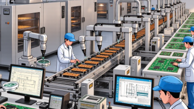
Surface-mount and through-hole components may be installed manually or with automated assembly equipment. |
Assembly verifies whether the fabricated board works with the intended components and production method. |
| Soldering |
Connection method |
Reflow soldering is commonly used for surface-mount components, while wave or selective soldering may be used for through-hole parts. |
The soldering method must match the component types, board materials, and assembly requirements. |
| Inspection |
Physical inspection |
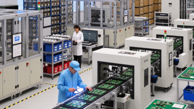
Inspection may include visual checks, dimensional measurement, automated optical inspection, and verification of solder joints. |
Inspection helps identify opens, shorts, insufficient solder, misalignment, and mechanical defects. |
| Electrical Testing |
Continuity and isolation |
Open-and-short testing checks whether intended conductive paths are continuous and unintended connections are absent. |
Electrical testing confirms basic board connectivity before functional evaluation. |
| Functional Testing |
Operating verification |
The assembled prototype is powered and tested under specified operating conditions, including interfaces, inputs, outputs, and communication functions. |
Functional testing determines whether the complete design performs as intended. |
| Prototype Iteration |
Engineering revision |
Test results may lead to changes in schematic design, PCB layout, component selection, thermal management, or enclosure fit. |
Several design-build-test cycles are common before a design is released for volume manufacturing. |
| Key Deliverable |
Validated design package |
A completed prototype normally produces updated design files, test records, assembly notes, and documented revision changes. |
Accurate documentation supports repeatability, certification activities, and future production. |