What Is PCB Board Assembly and How Does It Work?

Pcb Board Assembly is the practical bridge between an electronic design and a working product. It turns a bare circuit board into a functional device by placing components, forming electrical connections, and checking performance. The process may look mechanical, but small decisions can affect reliability, cost, and production speed.

As electronics manufacturing expert Happy Holden has stated, “The printed circuit board is the platform on which all electronic components are mounted.” His observation explains why assembly deserves careful attention. A board is not merely a flat sheet with soldered parts. It includes copper traces, surface-mounted devices, through-hole components, solder joints, inspection points, and sometimes complex thermal paths. Each part must cooperate.

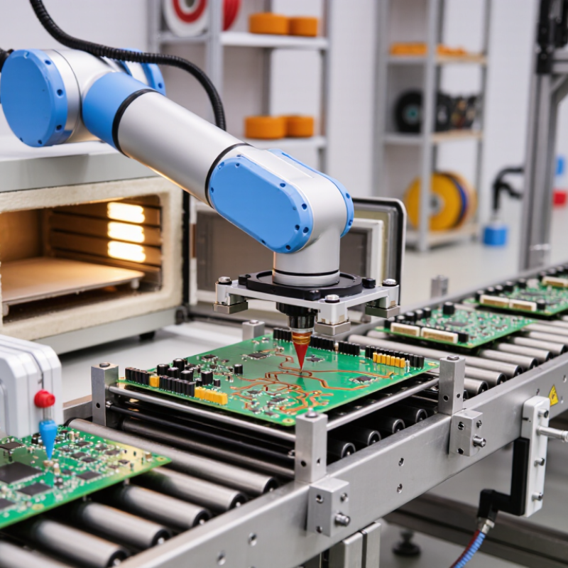
The workflow usually begins with material preparation and solder paste printing. Pick-and-place machines then position components with remarkable precision. Reflow ovens heat the board through controlled temperature zones. Larger or heavier parts may require selective soldering or manual installation. Automated optical inspection can reveal bridges, missing components, and misalignment. Functional testing offers another layer of evidence.

Still, the process is not flawless. A perfect-looking joint may hide a weakness. A clean inspection report cannot predict every field condition. Moisture, vibration, heat, and operator handling can expose unnoticed problems. That is why experienced manufacturers combine design rules, process control, inspection, and testing. This article examines how Pcb Board Assembly works, what each stage contributes, and where practical judgment remains essential.
What Is PCB Board Assembly and How Does It Work?

PCB Board Assembly: Definition, Purpose, and Core Components

PCB board assembly is the process of mounting electronic components onto a printed circuit board. The bare board provides electrical paths, while assembly turns it into a working circuit. Components may include resistors, capacitors, integrated circuits, connectors, sensors, and switches. Small parts often resemble grains of sand.

The main purpose is to create a reliable electrical connection in a compact, repeatable form. Assembly usually involves solder paste printing, component placement, soldering, inspection, and functional testing.

Surface-mount components sit directly on the board surface. Through-hole parts use leads inserted through drilled holes. Each method has practical advantages, and some boards require both.

Temperature control matters because excessive heat can damage sensitive components or weaken solder joints.

Core components include the PCB substrate, copper traces, solder pads, solder material, and electronic devices. A multilayer board may contain internal power and signal planes that cannot be seen after assembly.

Production teams check polarity marks, component values, alignment, and solder coverage. Automated optical inspection can reveal shifted parts, but it cannot confirm every electrical behavior. Testing remains necessary.

A board may look perfect and still fail under load.

Assembly drawings, approved component data, and controlled process records improve traceability and reliability. Yet mistakes still happen, especially when a similar-looking component is placed incorrectly.

That risk deserves review, not assumption. Good assembly depends on accurate design data, careful handling, and measured verification at each stage.


How a Printed Circuit Board Assembly Is Designed and Prepared

PCB board assembly begins long before components reach a production line. A designer turns the circuit diagram into a practical board layout. The work includes placing footprints, routing traces, defining copper layers, and checking electrical clearances. Component height matters near connectors and enclosures. Heat-producing parts need room for airflow or a thermal path. Small details matter. A first layout is rarely perfect, especially when the schematic misses a mechanical constraint.

Preparation continues with a complete bill of materials, approved component data, fabrication notes, and assembly drawings. The design team reviews pad sizes, polarity marks, reference labels, and the board stack-up. High-speed signals may require controlled impedance and carefully matched trace lengths. A design-for-manufacturing review can reveal narrow gaps, weak solder joints, or parts that cannot be placed reliably. These checks reflect practical production experience, not just software rules.

Before assembly, engineers export verified manufacturing files and compare them with the final revision. The assembler then programs placement equipment, prepares the solder paste stencil, and confirms feeder positions. A small sample build can expose reversed footprints, insufficient paste, or unexpected component interference. Not quite ready. Engineers should record every correction, inspect solder joints, and update controlled documents before larger production begins. Skipping one review may create expensive rework later.

The Step-by-Step Process of Placing and Soldering Components

PCB board assembly turns a bare circuit board into a working electronic unit. The process starts with a bill of materials, component verification, and solder-paste inspection. A stencil spreads paste onto copper pads. The layer must be even. Too much paste can create bridges between nearby pads.

A pick-and-place machine then positions resistors, capacitors, integrated circuits, and connectors. Fiducial marks help the camera correct board alignment. IPC process guidance commonly keeps placement accuracy within a few dozen micrometers for fine-pitch components. The board then enters a reflow oven. Controlled heating activates the flux, melts the solder, and forms electrical joints. A typical lead-free profile peaks near 240°C, although the component datasheet remains the controlling reference.

Larger parts may require selective soldering or hand soldering. Operators inspect joints using optical systems, while X-ray inspection checks hidden connections beneath grid-array packages. IPC-A-610 and J-STD-001 define widely used acceptance and soldering requirements. The World Semiconductor Trade Statistics Spring 2024 forecast projected semiconductor sales growth of 16.0% in 2024, increasing pressure on assembly lines and inspection capacity. Faster output is useful, but rushing the thermal profile can damage components. A perfect board is not produced by speed alone. Rework still happens. Careful records of paste volume, oven temperature, and inspection results make defects easier to trace. In practice, assembly quality depends on disciplined control at every small step, not only on expensive equipment.

Inspection, Testing, and Quality Control in PCB Assembly

PCB assembly combines bare boards, components, solder, and controlled heat into a working electronic product. Quality depends on more than visual appearance. Inspection, testing, and traceability must work together.

Solder paste inspection checks volume, height, and position before components are placed. Automated optical inspection then detects missing parts, polarity errors, bridges, and poor solder joints. X-ray inspection reveals hidden connections under packages. In-circuit testing measures electrical paths, while functional testing confirms real operating behavior.

IPC’s 2023 Global Sentiment of the Electronics Industry report identified supply continuity, material variation, and workforce capability as continuing industry pressures. These pressures can increase assembly risk. The ASQ Cost of Quality research commonly estimates poor quality may consume 15% to 20% of revenue in some organizations. That figure is not universal, but it explains why early detection matters.

Tips: Define acceptance criteria before production. Record inspection images, operator actions, lot numbers, and rework decisions. Use statistical process control for solder volume and placement accuracy. Do not treat automated inspection as infallible. False calls can hide real problems when teams rush. A small sample of boards should receive deeper review, especially after a component or supplier change. IPC-A-610 workmanship criteria can support consistent judgment, but engineers should still examine unusual defects. Real factories are imperfect. A clean report does not always mean a reliable product. Reflection after failures is still part of quality control.

Common PCB Assembly Methods and Their Practical Applications

PCB board assembly turns a bare circuit board into a working electronic unit. It involves placing components, connecting them, and checking every joint. The chosen method depends on component size, product volume, and mechanical stress.

Surface-mount technology, or SMT, places small components directly on copper pads. It suits compact devices, control panels, and high-volume production. A stencil spreads solder paste across the board. Pick-and-place equipment positions components accurately. A reflow oven then melts the paste. Through-hole assembly uses component leads inserted through drilled holes. Solder fills the opposite side and creates strong mechanical connections. This method works well for power supplies, industrial controls, and connectors exposed to vibration. It is slower, but often more durable.

Mixed assembly combines SMT and through-hole parts on one board. It is practical when a product needs both compact circuits and sturdy connectors. Inspection may include visual checks, automated optical inspection, and electrical testing. No method is perfect. Small solder bridges can escape a rushed inspection.

Tips: Match the assembly method to the product’s real working conditions. Check pad design, component spacing, and heat tolerance before production. Keep moisture-sensitive parts sealed and handle boards with grounded equipment. A prototype may pass basic testing but fail after repeated heating cycles. Record defects carefully, then adjust the stencil, solder profile, or placement settings. Tiny changes matter.

What Is PCB Board Assembly and How Does It Work? - Common PCB Assembly Methods and Their Practical Applications
Assembly Method How It Works Typical Components Production Volume Main Advantages Key Limitations Practical Applications
Surface-Mount Technology (SMT) Solder paste is applied to PCB pads, components are accurately placed on the surface, and the board passes through a reflow oven to melt and solidify the solder. Resistors, capacitors, integrated circuits, diodes, transistors, connectors, and other surface-mount devices. Medium to high High placement speed, compact layouts, good electrical performance at high frequencies, and efficient automated production. Requires accurate placement equipment and thermal process control; some components are difficult to inspect or repair manually. Consumer electronics, computing equipment, telecommunications, industrial controls, and automotive electronics.
Through-Hole Technology (THT) Component leads are inserted through drilled holes in the PCB and soldered to pads on the opposite side. Large connectors, transformers, switches, relays, power components, and mechanically stressed components. Low to medium Strong mechanical attachment, easier manual inspection, and good suitability for larger or heavier components. Requires drilled holes, uses more board area, and generally supports lower component density than SMT. Power supplies, industrial equipment, instrumentation, audio equipment, and products exposed to vibration.
Mixed Technology Assembly SMT and THT components are combined on one PCB, usually with reflow soldering for SMT parts followed by wave, selective, or hand soldering for through-hole parts. A combination of compact integrated circuits and larger connectors, power devices, or mechanical components. Low to high Balances compact design, electrical performance, component strength, and broad component compatibility. Requires multiple process stages, careful thermal planning, and more complex inspection and rework procedures. Industrial controllers, measurement systems, networking equipment, automotive modules, and complex consumer products.
Manual or Hand Assembly Operators place and solder components using hand tools, soldering irons, hot-air tools, or microscopes. Prototype parts, unusual packages, sensitive components, repair parts, and low-volume components. Prototype to low Flexible, low setup cost, suitable for engineering changes, and practical for prototypes or difficult-to-automate parts. Slower production, higher variation between operators, and greater risk of soldering or placement errors. Engineering prototypes, product development, repairs, laboratory equipment, and small customized batches.
Reflow Soldering A controlled temperature profile heats solder paste until it melts, wets the component leads and pads, and forms solder joints during cooling. Primarily SMT components, including fine-pitch packages and miniature passive components. Medium to high Repeatable solder joints, high throughput, precise thermal control, and compatibility with automated SMT lines. Improper profiles can cause tombstoning, insufficient wetting, voids, warpage, or thermal damage. Most modern electronic products using predominantly surface-mounted components.
Wave Soldering The underside of a populated PCB moves across a controlled wave of molten solder, connecting exposed through-hole leads and selected solderable areas. Through-hole components and suitable bottom-side solder joints; some mixed-technology boards. Medium to high Fast and consistent soldering for many through-hole joints with relatively low labor requirements. Less suitable for densely populated boards, fine-pitch parts, and components that cannot tolerate the solder wave or heat. Power electronics, control boards, appliance electronics, and boards with many through-hole components.
Selective Soldering A programmable solder nozzle applies molten solder only to specified through-hole locations after other components have been assembled. Through-hole components on mixed-technology boards, especially near sensitive SMT components. Low to medium Reduces masking requirements, limits thermal exposure, and provides controlled soldering for targeted joints. Equipment programming and fixturing can add process time and cost, particularly for small or frequently changing batches. Automotive electronics, industrial controls, power conversion equipment, and complex mixed-technology assemblies.
Automated Optical Inspection (AOI) Cameras compare the assembled PCB with programmed inspection criteria to detect placement, polarity, solder, and component defects. Surface-mount and selected through-hole components, solder joints, markings, and component orientation. Medium to high Fast non-contact inspection, repeatable results, and early detection of common assembly defects. May produce false calls, cannot verify every hidden solder joint, and requires properly prepared inspection programs. SMT production lines, mixed-technology assembly, process monitoring, and quality control.
X-Ray Inspection X-rays penetrate the assembly to create images of hidden solder joints and internal structures that are not visible from the surface. Ball-grid arrays, bottom-terminated components, hidden-pad packages, multilayer solder joints, and void-sensitive connections. Low to high Detects hidden defects such as voids, opens, insufficient solder, shorts, and misalignment beneath packages. Higher equipment cost, slower inspection than basic visual checks, and the need for trained interpretation. High-reliability electronics, power modules, advanced computing hardware, aerospace-related systems, and medical equipment.
Process Overview: A typical PCB assembly workflow includes design-for-manufacturing review, component sourcing, solder-paste printing, component placement, soldering, inspection, testing, and final rework or packaging when required. The selected method depends on component type, board complexity, production volume, reliability requirements, and cost targets.